The tie cell is a standard cell, designed specially to provide the high or low signal to the input (gate terminal) of any logic gate. The high/low signal can not be applied directly to the gate of any transistors because of some limitations of transistors, especially in the lower node. The limitation will also be discussed along with the schematic and operation of tie cells in this article. We will discuss the following sub-topics in this article.
- Need of tie cells
- Schematic of tie cells
- The function of tie cells
- Placement of tie cells
Need of tie cells:
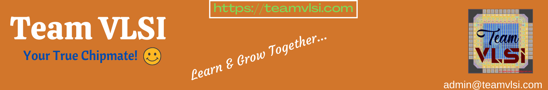
In the lower technology node, the gate oxide under the poly gate is a very thin and the most sensitive part of the transistor. We need to take special care of this thin gate oxide while fabrication (associated issue is antenna effect) as well as in operation too. It has been observed that if the polysilicon gate connects directly to VDD or VSS for a constant high/low input signal, and in case any surge/glitch arises in the supply voltage it results in damage of sensitive gate oxide. To avoid the damages mentioned above, we avoid the direct connection from VDD or VSS to the input of any logic gates. A tie cell is used to connect the input of any logic to the VDD or VSS.
 |
| Figure-1: Need of tie cell |
There are two types of tie cells.
- Tie-high cell
- Tie- low cell
As the name suggests, the tie-high cell’s output is always high and the tie-low cell’s output is always low.
Schematic of tie cells:
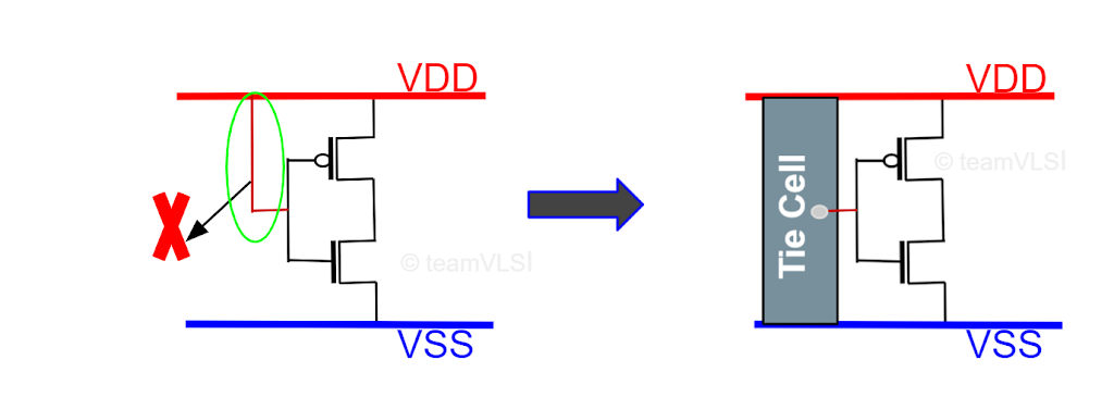
The tie cell has no input pin and only one output pin. The output of the tie-high cell is always high and the output of the tie-low cell is always low and it is the glitch-free output that connects to the input of any logic gates. The schematic of tie high cell and tie-low cell is shown in the figure-2.
 |
| Figure-2: Tie-high and tie-low cells |
In the tie-high cell, the drain and gate of nMOS are shorted together and connected to the gate of pMOS, and output is taken from the drain of pMOS. Whereas in the tie-low cell the drain and gate of pMOS are shorted together and connected to the gate of nMOS and output is taken from the drain of nMOS. The function of these schematics is explained in the next section.
Function of tie cells:
Both tie-high and tie-low cells have similar working. Here working of the tie-high cell is explained. A similar logic can think for tie-low cell. From figure-2 tie-high cell, the drain and gate of nMOS are shorted.
So Vg = Vd
==> Vgs = Vds
Therefore, Vds > Vgs -Vt
This shows that the nMOS will always be in the saturation region. The configuration of MOS where drain and gate are shorted is popularly known as a diode-connected transistor. And when nMOS is behaving like a diode here, the gate of pMOS is always low and so pMOS is always in on state. When pMOS is in on state its drain which is output will always be high.
Similarly, for the tie-low cell, the pMOS is always in saturation region so the gate of nMOS is always high and hence the drain of nMOS will always be at the low logic.
One more important thing is here that the sudden spike in VDD or VSS will be not propagated to the output of the tie cell.
Placement of tie cells:
Tie cells are not present in the synthesized netlist and not placed in the initial placement of the standard cells. Tie cells are inserted in the placement stage and more specifically at the final stage of placement. Where ever netlist is having any pin connected to 0 logic or 1 logic (like .A(1’b0) or .IN(1’b1), a tie cell gets inserted there. Click here to read more about the placement stage and the order where the tie cell get inserted in the placement stage.