
Electromigration is an important issue especially in lower technology node where the cross-sectional area of metal interconnects is very less. In this article, we will discuss the phenomenon of electromigration, the effects of electromigration and the ways to prevent the electromigration issue.
Electromigration:
When a high current density passes through a metal interconnect, the momentum of current-carrying electrons may get transferred to the metal ions during the collision between them. Due to the momentum transfer, the metal ions may get drifted in the direction of motion of electrons. Such drift of metal ions from its original position is called the electromigration effect.
Current density J is defined as the current following per unit cross-section area.
J = I/A
Where I is the current and A is the cross-section of the area of interconnect.
As the technology node shrinks, Cross-sectional area of the metal interconnects also shrinks and the current density increases in great extent in the lower node. Electromigration has been a problem since 90 nm technology node or even earlier but it gets worse in lower technology node 28nm or lower node.
Electromigration Phenomenon:
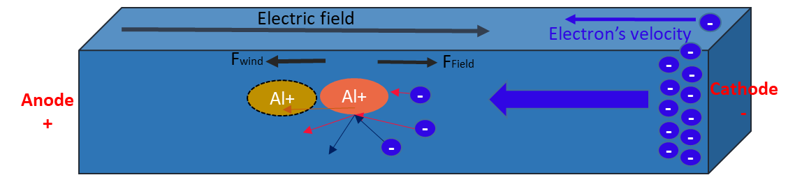 |
| Figure-1: Electromigration phenomenon |
Figure-1 shows the phenomenon of electromigration effect. A potential difference is applied across a metal interconnect which setups an electric field from anode side to cathode side as shown. This electric field causes to move the electron in the opposite direction of the electric field. This momentum of electron cause flow of current in the electron. These moving electrons have momentum and when it collides with the metal ions the metal ions feel two forces in the opposite direction as shown in the figure. One force and due to electric field and other is due to strike of electrons wind. If the current density is high the force due to electron wind is greater than the force due to the electric field.
Depending on the current density, the subjected metal ion started drifting in the opposite direction of the electric field. If the current density is high, the interconnect may get affected of EM instantly or some times the effect may come after months/years of operation depending on current density. So the reliability of ASIC will depend upon this EM effect.
Mean Time To Failure (MTTF) is an indication of the life span of an integrated circuit. MTTF is calculated using Black’s equation as bellow.
Where A = Cross-Section area
J = Current density
N = Scaling factor (normally set to 2)
Ea = Activation energy
K = Boltzmann’s constant
T = Temperature in Kelvin
Effects of EM:
Once the metal ions get started to shifting from its original position, these will create problems in the interconnect. It could result in an excess of ions accumulation in a particular location of deficient of ions. So either Hillocks or Void could occur in the metal interconnect.
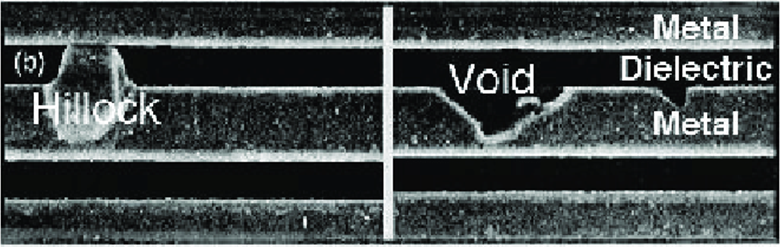 |
Figure-2: Hillock and Void formation in Interconnect |
Figure-2 shows the formation of hillocks and void.
Void: If the incoming ion flux is lesser than the outgoing ion flux, It will create a void in interconnect. A void can lead a discontinuity in the interconnect and result an open circuit.
Hillocks: If incoming ion flux is greater than the outgoing ion flux, It will cause the accumulation of ions and create a hillock in the interconnect. A hillock can increase the width of a metal interconnect and touch the neighbouring metal interconnect which may result in a short circuit.
Prevention techniques for EM:
With the scaling of the technology node, the interconnect used is also changed. Initially, pure Aluminium was used as interconnect then the industry started using the Al-Cu alloy and later shifted to Copper interconnects. Copper interconnects can withstand approximately 5 times more current as compared to Aluminium interconnects while maintaining similar reliability requirements.
During the physical design, the following techniques could be used to prevent the EM issue.
- Increase the metal width to reduce the current density
- Reduce the frequency
- Lower the supply voltage
- Keep the wire length sort
- Reduce the buffer size in clock lines
To prevent the EM issue, EM Checks is performed during the physical signoff stage with respect to the EM rules provided by the foundry.
Thank You!