
Before discussing the prevention techniques of Latch-up issue, let’s recall the key factor of the latch-up issue first. The following two factors are important for the latch-up issue.
- High resistance of n-well and p-substrate
- β1 x β2 > 1
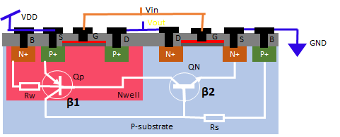
Figure-1 shows the parasitic BJT formation which causes latch-up. n-well and p-substrate resistance can be reduced by increasing the doping but it will degrade the device performance drastically. But we can cut down the gains of parasitic BJT (β) and prevent the latch-up issue. Some popular techniques for latch-up prevention are as below.
- Guard ring
- Well tap cells
- Isolation trench
- Epitaxial layer
- Retrograde well doping
- Combination of epitaxial layer and retrograde well doping
- FDSOI Technology
- ESD protection techniques
1. Guard ring:
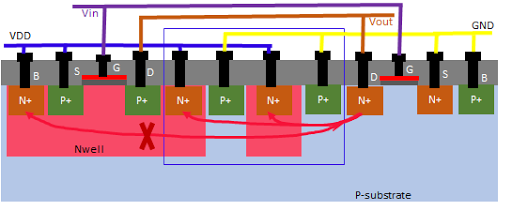
If Vout goes bellow the VSS and the diode between drain and p-substrate of nMOS become forward bias, electrons from drain start injecting from to substrate and collected by the body of pMOS. This cause a current from in the opposite direction of electron flow. which ultimately triggers the Qp transistor as shown in the figure-1. Now to break this chain, two sets of n+ implant in n-well, p+ implant on p-substrate added in between nMOS and nMOS as shown in the figure-2. These will collect the electrons injected from the drain of nMOS and prevent the current flow from the drain of nMOS to the body of pMOS. Which stops triggering the Qp BJT.
Similarly in case of the Vout goes above the VDD and drain of pMOS start injecting holes in n-well and goes and collected by the body of nMOS. This lead to the trigger of Qn BJT. But by adding the guard ring these holes will be collected by the guard ring and stop the latch-up.
2. Well tap cells:
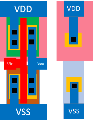
In tapless standard cell design to prevent the latch-up, we need to tap the n-well to VDD and p-sub to VSS. These well tap cells tap the n-well to VDD and p-sub to VSS. Figure-3 shows the crosssection of tapless cell and figure-4 show the layout of well tap cell and tapless standard cell.

The well tap cells are placed in the standard cell row in the regular interval as per the maximum distance rule define in technology library.
3. Oxide trench isolation:
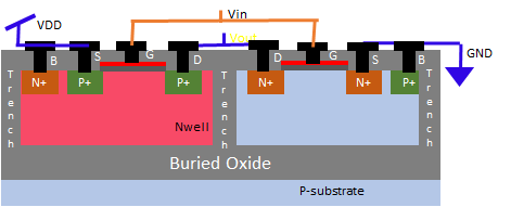
In this technique, nMOS and pMOS have insolated using the buried oxide and oxide trench. A horizontal buried oxide created deep inside and vertical oxide trenches are created later and connected both together to separate the n-well and p-substrate. The oxide trenches are isolator in nature so oxide trench stops the formation of the PNPN device. A cross-section of oxide trench isolation is shown in the figure-5.
4. Epitaxial Layer:
In this technique, a low doped p-epitaxial layer (known as P-) grown over the P-substrate (called P+). The P- epitaxial layer provides a low impedance path for minority carrier which prevents the latch-up triggering. This technique is also called P on P+. A cross-section epitaxial layer has shown in the figure-6.
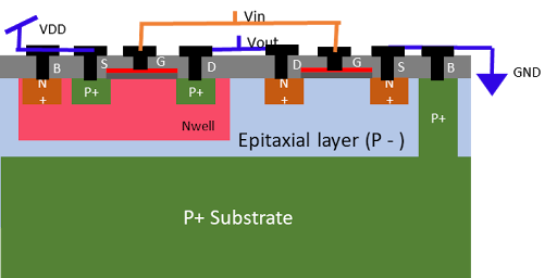
The only problem with this technique is, it’s a sophisticated process to grow the epitaxy layer. Another alternative is we can use the epitaxy wafer for this purpose.
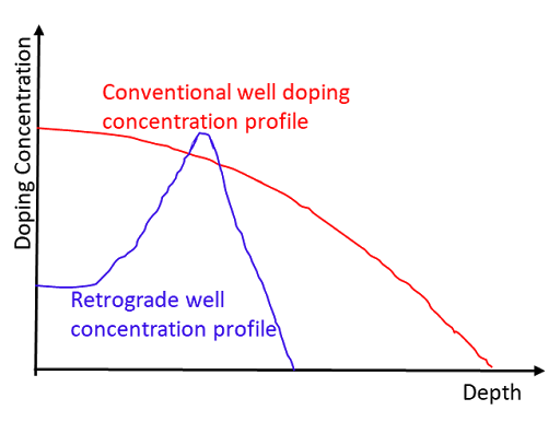
5. Retrograde Well Doping :
In normal n-well doping process, the doping concentration is highest at the surface and it decreases as the depth of well increases. But in the retrograde well doping process, there is very precise control of doping concentration over the depth and we have peak doping concentration at deep inside the n-well, not at the surface. A doping profile of normal doping and retrograde well doping is shown in figure-7.
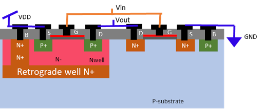
A retrograde well doping is done at the bottom of normal n-well as shown in the figure-8. This region has a high doping concentration and creates a low resistance path. The body connection which is taken from N+ doping is extended to this high dopped region. So there is the formation of low resistive path bellow the n-well which stops the triggering of PNPN device. A cross-section view of retrograde well doping has shown in figure-8.
6. Combination of the epitaxial layer and retrograde well doping :
We can use a combination of the epitaxial layer and retrograde well doping together both the techniques together which is also a very effective way to prevent the latch-up issue but the process is a bit complex.
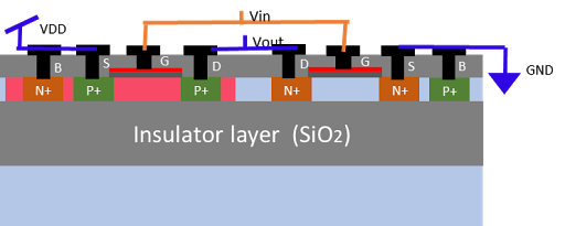
7. SOI Technology :
In SOI (Silicon on Insulator) technology an oxide layer comes bellow the source-drain doping and stop the parasitic BJTs formation. So SOI technology completely eliminates the latch-up issue. A cross-section of CMOS in SOI technology has shown in figure-9.
We can use a combination of the epitaxial layer and retrograde well doping together both the techniques together which is also a very effective way to prevent the latch-up issue but the process is a bit complex.
These are the ways to prevent latch-up in CMOS technology. Each technique has its own pros and cons.
Thank You!